 ISSN: 2822-0838 Online

Bismuth Coated Screen-printed Electrode Platform for Greener Anodic Stripping Voltammetric Determination of Cadmium and Lead
Autchara Paukpol and Jaroon Jakmunee*Published Date : 2019-08-23
DOI : 10.12982/cmujns.2016.0007
Journal Issues : Number1 ,January - April 2016
ABSTRACT
A greener electrochemical platform was developed to determine trace amounts of cadmium and lead. It is based on a disposable screen-printed carbon ink electrode modified with an in situ plated bismuth film employed as a more environmentally-friendly working electrode alternative to the widely used mercury electrode. The bismuth coated screen-printed electrode (Bi-SPE) was used for the simultaneous determination of trace Cd(II) and Pb(II) by squarewave anodic stripping voltammetry (SWASV). Operational parameters such as Bi(III) concentration, deposition potential, deposition time and rotation speed during preconcentration of the metals were optimized. The Bi-SPE presented well-defined, reproducible, and sharp stripping voltammograms. Peak current increased linearly with the metal concentration in a range of 5-40 μg L-1 for Cd(II) and 2-40 μg L-1 for Pb(II). The limits of detection were 1.7 μg L-1 for Cd(II) and 0.7 μg L-1 for Pb(II), which are better than those of the flame atomic absorption method. The proposed method was successfully applied to determine trace cadmium and lead in river water samples. Accuracy of the developed method was examined by spiking Cd(II) and Pb(II) standard solutions into river water samples, and percentage recoveries were obtained in the range of 86.4-110.6%. The SWASV with the new Bi-SPCE electrode provided advantages, including high sensitivity, low detection limits, low background current, portability, fast and cost-effective determinations, and, importantly, the use of relatively non-toxic chemicals.
Keywords: Bismuth coated screen-printed electrode, Square-wave anodic stripping voltammetry, Cd(II), Pb(II), Water samples
INTRODUCTION
The growing concerns about Cd(II) and Pb(II) poisoning have led to increasing demands for highly sensitive, reliable, reproducible, and low cost methods for quantitation in water. Electrochemical stripping analysis has been recognized historically as a powerful technique for Cd(II) and Pb(II) detection. In stripping voltammetry, the mercury film or hanging mercury drop electrode (MFE/HMDE) has been widely applied as a working electrode owing to its remarkable sensitivity. However, the toxicity of mercury has stimulated the search for environmentally-friendly material to produce a greener, mercury-free electrode. The bismuth film electrode (BiFE) is considered the best alternative to MFE due to its ability to form fusing alloys with other metals (Wang et al., 2000; Locatelli and Torsi, 2001 and Arduini et al., 2010). Different materials have been used as substrates for BiFEs, including glassy carbon (Wang et al., 2001a and Kefala et al., 2003), carbon paste (Krolicka et al., 2002 and Svancara et al., 2003), wax-impregnated graphite (Kefala et al., 2003), pencil-lead (Demetriadis et al., 2004), and screen-printed carbon ink (Wang et al., 2001b). Screen-printing technology is well established for the production of low-cost, reproducible, and sensitive electrochemical sensors. Screen-printed sensors have been widely used for environmental, biomedical, and industrial monitoring (Goldberg et al., 1994 and Laschi et al., 2006).
In this study, bismuth film was screen-printed in situ carbon working electrodes and used in square wave anodic stripping voltammetry (SWASV) to determine Cd(II) and Pb(II) in water samples; the optimization, characterization and attractive analytical performance of bismuth coated screen-printed electrode was also reported.
MATERIALS AND METHODS
Chemicals and reagents
All the chemicals were of analytical reagent grade. Ultrapure water (Milli-Q water, resistivity of 18.2 MΩ cm-1) obtained from a Millipore water purification system (Millipore, Sweden) was used throughout. The solutions of Bi(III) (Carlo Erba, Italy), Cd(II) (Fluka, Switzerland) and Pb(II) (Merck, Germany) were prepared from 1000 mg L-1 standard solutions by appropriate diluting with Milli-Q water. An acetate buffer solution (0.1 M, pH 4.5) was prepared by mixing the acetic acid (Lab Scan, Thailand) and sodium acetate (Carlo Erba, Italy) and served as a supporting electrolyte.
Apparatus
Voltammetric measurements were performed with a Metrohm model 757 VA computrace with GPES software for control of the voltammograph linked with a personal computer. A bismuth coated screen-printed carbon electrode served as the working electrode, with the Ag/AgCl (3 M KCl) and platinum wire as the reference and counter electrodes, respectively. Plasma cleaner (PDC-32G, Harrick Plasma, USA) was used to pretreat the working electrode.
Bismuth coated screen-printed carbon electrode (Bi-SPCE) preparation
SPCEs were produced with a homemade manually screen-printing apparatus (Upan et al., 2015). Carbon ink (Henkel, Germany) was used to print the working electrode. The substrate was a flexible polyester film. The diameter of the working electrode was 3 mm. SPCEs were modified with bismuth using the in situ plating approach. Firstly, SPCEs were cleaned by subjecting them to air plasma in a chamber of the plasma cleaner. The chamber was evacuated to 0.15 torr and the plasma was generated at low frequency RF level. Then, the chamber was backfilled with air and operated at pressure 0.4 torr for 60 s. The plasma treated SPCEs were electrochemically treated in a 0.1 M acetate buffer solution at pH 4.5 by applying a positive potential of +1.6 V vs Ag/AgCl for 120 s, followed by +1.8 V vs Ag/AgCl for 60 s, and then thoroughly rinsed with water.
Measurement procedure
The electrochemical deposition on SPCEs coated by bismuth was carried out according to the following in situ procedure in the presence of dissolved oxygen. The SPCE was immersed in an electrochemical cell containing the specified concentration of Bi(III) in an acetate buffer (0.1 M, pH 4.5) medium and Bi was deposited on the metals on the surface of the electrode for a specified time while the solution was stirred. The analytical measurement used the square wave anodic stripping voltammetric mode (SWASV). ASV experiments consisted of three conventional steps: time controlled electrochemical deposition with solution stirring, rest period, and a positive voltammetric stripping scan under the selected conditions. The optimum conditions for SWASV method were as follows: frequency (f), 35 Hz; step potential (Estep) 4 mV; square wave amplitude 40 mV; deposition potential (Edep) -0.9 V; deposition time (tdep) 180 s; the potential scanning range from -0.9 to 0.3 V; equilibrium time (teq) 15 s; cleaning potential (Eclean) 0.3 V; and cleaning time 30 s. During the electrodeposition and precondition steps, the solution was stirred at 2000 rpm. In the analysis, an in situ plated Bi-SPE was prepared by adding the Bi solution to a water sample diluted in 0.1 M acetate buffer solution pH 4.5 to obtain 1 mg L-1 Bi(III) in the final solution. Calibration graphs were used to quantify Cd(II) and Pb(II) in natural water samples.
Analysis of real samples
Water samples were collected from the Ping River, Chiang Mai, Thailand at the sampling sites shown in Figure 1. Water samples were filtered through a 0.45 μm membrane. In the analysis, in situ plated Bi-SPCEs were prepared by spiking the sample with 1 mg L-1 Bi(III) in 0.1 M acetate buffer at pH 4.5. Calibration curves were used to quantify Cd(II) and Pb(II) in the samples.
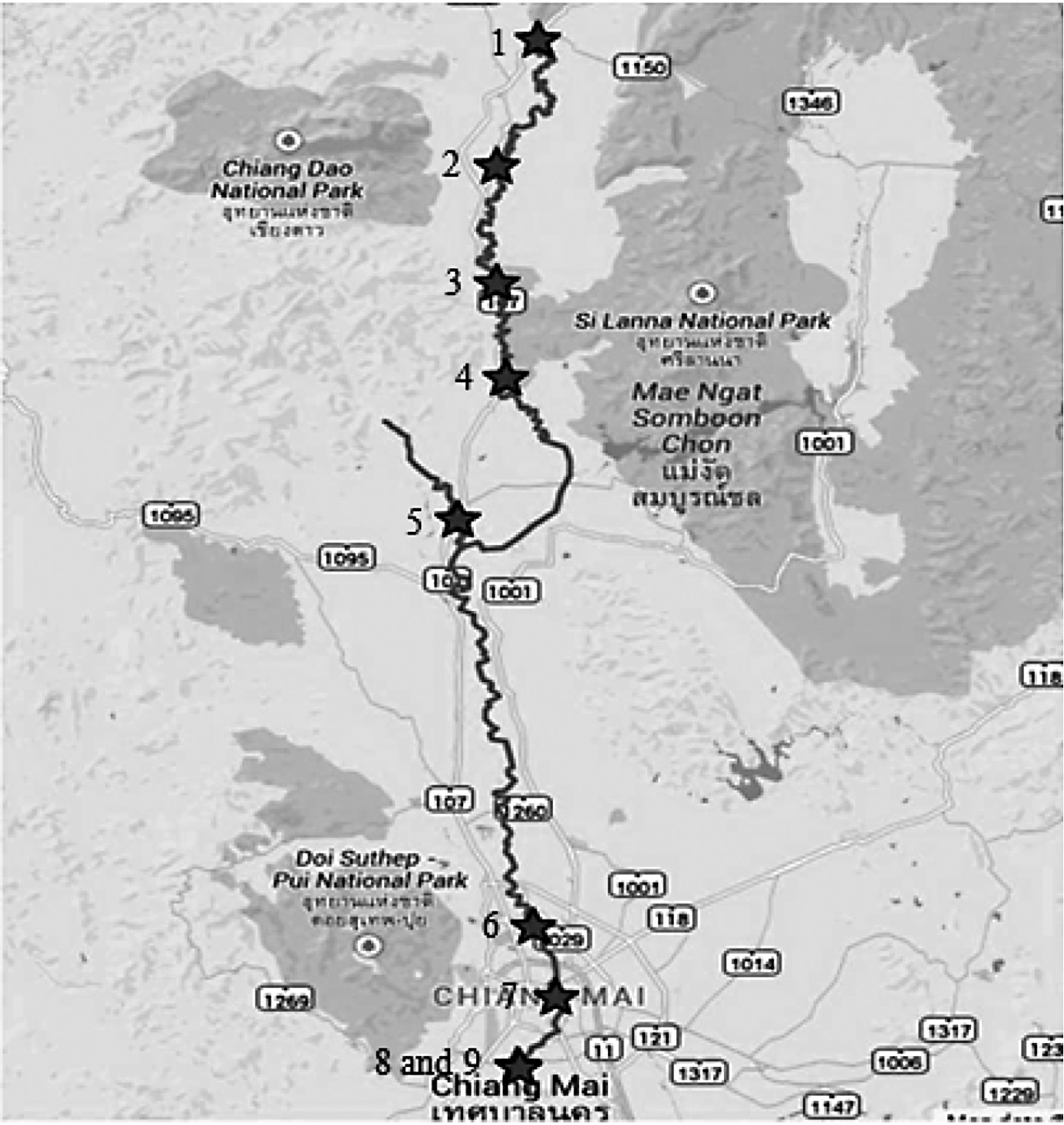
Figure 1. The water sampling sites in the Ping River, Chiang Mai, Thailand.
RESULTS
Effect of experimental variables
Bi(III) concentration. Representative Cd(II) and Pb(II) peak currents for a solution containing 100 μg L-1 each of Cd(II) and Pb(II) in 0.1 M acetate buffer
(pH 4.5) on in situ plated Bi-SPCEs with different Bi(III) concentrations in the range 100-1400 μg L-1 are shown in Figure 2(a).
Deposition potential. The effects of deposition potentials in the range of -0.75 to -1.60 V on the stripping currents of Cd(II) and Pb(II) are shown in Figure
2(b); the peak potentials for Cd(II) and Pb(II) were at -0.75 and -0.50 V as Ag/AgCl, respectively.
Deposition time. The effects of metal deposition times in the range of 60-420 s for the solution containing 100 μg L-1 each of Cd(II) and Pb(II) in 0.1 M acetate buffer (pH 4.5) are shown in Figure 2(c).
Rotation speed during preconcentration step. The effects of rotation speeds of the stirrer in the range of 0-3000 rpm are shown in Figure 2(d).
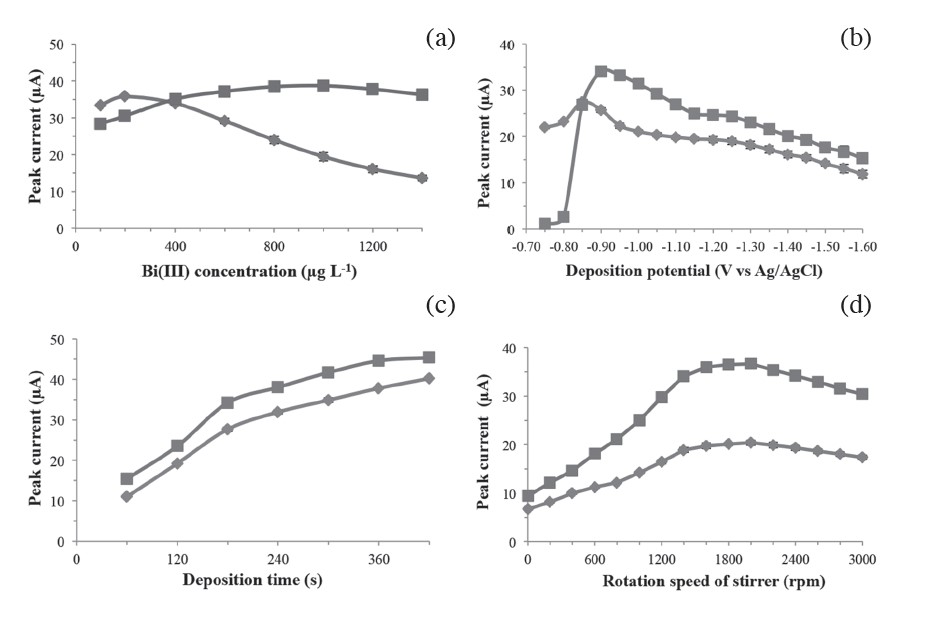
Figure 2. Effects of the Bi(III) concentration (a), deposition potential (b), deposition time (c), and rotation speed during preconcentration (d) on the stripping peak currents of Cd(II)  and Pb(II)
  in 100 μg L-1Cd(II) and Pb(II) with 0.1 M acetate buffer pH 4.5 using in-situ prepared Bi-SPCE, n = 3. SWASV parameter; step increment 4 mV, frequency 35 Hz, pulse height 40 mV, cleaning potential 0.3 V, and cleaning time 30 s.
Calibration data
Calibration was performed on Bi-SPCEs for the simultaneous determination of Cd(II) and Pb(II) by SWASV; the results are shown in Figure 3. A small background current over a wide potential range was noticed. Calibration graphs had different slopes in the ranges of 5-40 and 40-100 μg L-1 for Cd(II) and 2-40 and 40-100 μg L-1 for Pb(II), respectively. This may be a result of the limited surface area of the electrode, leading to the saturation of metals deposited on the electrode. At lower concentrations, the metals might disperse more on the electrode surface; on the other hand, at higher metal concentrations, they might deposit upon the previously deposited layer. The current obtained in the stripping step was directly proportional to the rate of oxidation of the metals back into the solution, which was related to the amounts of metals on the surface of the electrode. The analytical sensitivities were Cd(II): 1.21, 0.17 μA per μg L-1 (R2 = 0.9995, 0.9911) and Pb(II): 1.21, 0.15 μA per μg L-1 (R2 = 0.9961, 0.9959). On the same electrode, the relative standard deviations were 7.0% for Cd(II) and 5.8 % for Pb(II) at 20 μg L-1 level (n=15). The same SPCE electrode could be used for at least 15-20 stripping cycles without loss of sensitivity. The limits of detection were calculated, at a deposition time of 180 s, as 1.7 μg L-1 for Cd(II) and 0.7 μg L-1 for Pb(II).
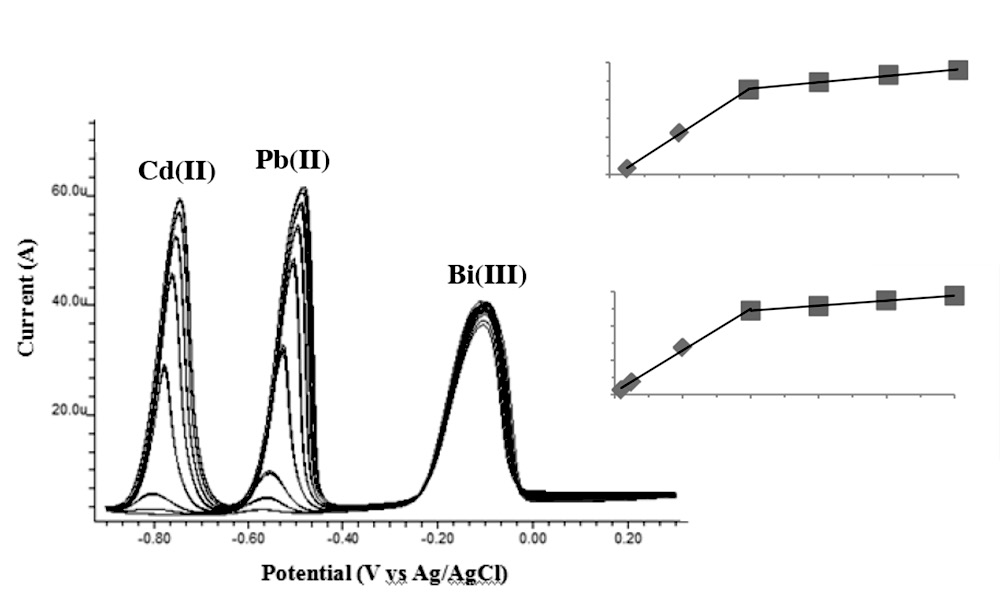
Figure 3. A series of voltammograms and calibration graphs for increasing concentrations of Cd(II) and Pb(II) in 0.1 M acetate buffer pH 4.5 using in-situ prepared Bi-SPCE (1 mg L-1 Bi(III)), n = 3. SWASV parameter; deposition potential -0.9V vs Ag/AgCl, deposition time 180 s, stirrer speed 2000 rpm, step increment 4 mV, frequency 35 Hz, pulse height 40 mV, cleaning potential 0.3 V and cleaning time 30 s.
Accuracy of the method
The system accuracy was determined by spiking water samples with Cd(II) and Pb(II) standard solutions of 5 μg L-1 and measuring the percent recoveries of Cd(II) and Pb(II). The results are given in Table 1. Percent recoveries of Cd(II) and Pb(II) are close to 100%, in the range of 86.4 to 110.6%, under the optimal condition.
Application to river water
For the purpose of practical applicability, Bi-SPCEs were employed to determine Cd(II) and Pb(II) in river water samples. The anodic stripping peak current was recorded with the calibration graph method under optimized conditions for determining Cd(II) and Pb(II). The results obtained for nine water samples are summarized in Tables 1 and 2.
Table 1. Determination of Cd(II) in water samples by the proposed SWASV with Bi-SPCE.
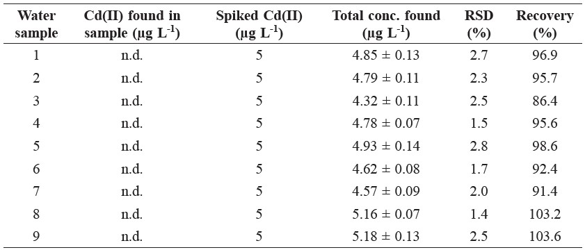
Note: * n.d. = not detectable.
Table 2. Determination of Pb(II) in water samples by the proposed SWASV with Bi-SPCE
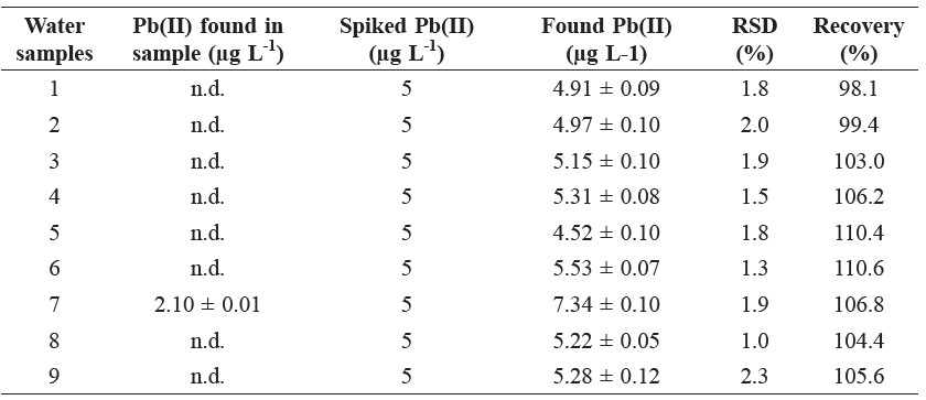
Note: * n.d. = not detectable.
DISCUSSION
The concentration of Bi(III) is a key parameter, as it controls the thickness of the Bi film; the thickness of the film does not affect the peak potential of any metals, but rather the peak height. The results showed a decrease of peak current of the Cd(II) and Pb(II) with increasing thickness of the Bi film, especially the Pb(II) peak, as shown in Figure 2(a). Since Pb(II) has a more positive reduction potential than Cd(II), Pb(II) can be determined at lower Bi(III) concentrations. At high Bi(III) concentrations, the peaks became wider and led to a substantial decrease in sensitivity at Bi(III) concentrations over 1000 μg L-1, due to a saturation effect of the Bi film on the screen-printed carbon surface. This behavior is attributed to the increased number of nucleation sites and increased alloy formation. However, at Bi(III) concentrations greater than 1000 μg L-1, a reduction in the peak intensity was observed, ascribed to the formation of a thick layer of Bi on the electrode surface that partially blocks the conductive surface of the electrode, reducing the number of electroactive sites (Kachoosangi et al., 2007). Thus, a Bi(III) concentration of 1000 μg L-1 was selected for further experiments.
The deposition potential affects the quality of bismuth film to form fused alloys with reduced metal ions. As shown in Figure 2(b), the stripping responses of Cd(II) and Pb(II) were found to occur at potentials more negative than -0.75 V. As the deposition potential became more negative, the peak currents increased up to -0.90 V for Cd(II) and -0.85 V for Pb(II). The Pb(II) peak current did not increase significantly from -0.75 to -0.85 V, due to its more positive reduction potential relative to Cd(II). The evolution of hydrogen gas from the SPCE surface that started to occur at -1.50 V could damage the bismuth film, and some interfering species may be deposited on the electrode at more negative potential. Therefore, a potential of -0.9 V was chosen as the optimal deposition potential.
The deposition time is the time required for Bi-SPCE to reduce Cd(II) and Pb(II) to Cd(Bi) and Pb(Bi) alloys, respectively. It is generally accepted that lower limits of detection (LODs) can be obtained with longer deposition times (Castaneda et al., 2005). In Figure 2(c), Cd(II) and Pb(II) peak currents increased rapidly with deposition times from 60-180 s. For deposition times longer than 180 s, the current responses increased negligibly, so this was considered the longest practical time for a satisfactory compromise between high sensitivity and short analytical times. Metal ions were preconcentrated for 180 s in further experiments.
The rotational speed of the stirrer controlled the mass transport behavior during the preconcentration step, as shown in Figure 2(d). The stripping peak currents for Cd(II) and Pb(II) continuously increased with each increment of rotational speed up to 2000 rpm. Beyond 2000 rpm, peak currents decreased because the bismuth film may have become mechanically damaged; therefore, preconcentration was performed at 2000 rpm.
The SWASV with bismuth film working electrode can simultaneously determine trace amounts of Cd(II) and Pb(II) in real water samples using calibration graphs. This method was highly sensitivitysensitive, consumed low amounts of reagent and sample, and was convenient to operate. It was also able to determine both metals in water samples at concentrations lower than the detection limits of the standard FAAS method. In comparison to the FAAS method, the developed voltammetric method was more sensitive with lower detection limits, less costly, and consumed fewer chemicals and energy (Roongjang et al., 2014).
The proposed method successfully analyzed real water samples, with recovery rates in the range of 86.4 to 110.6%. The results obtained for nine water samples are summarized in Table 1. The concentrations of the investigated metal ions in the Ping River water were very low and should have no environmental impact. According to the Thailand Pollution Control Department (PCD) Water Quality Standards, the maximum acceptable concentrations for Cd(II) and Pb(II) in drinking water are 10 μg L-1 and 50 μg L-1, respectively. The developed method can be used for monitoring these trace metals in natural water sources. The proposed Bi-SPCE was more environmentally friendly than the mercury-based electrode. Moreover, the screen-printed carbon electrode is conveniently fabricated, less expensive, and can be mass produced, as compared to other carbon electrodes, such as glassy carbon (Wang et al., 2001a; Kefala et al., 2003), carbon paste (Krolicka et al., 2002; Svancara et al., 2003), and wax-impregnated graphite (Kefala et al., 2003).
CONCLUSION
The developed anodic stripping voltammetric method with in situ coated Bi film on screen-printed carbon working electrode offers a cost-effective and sensitive alternative analytical method for the simultaneous determination of trace Cd(II) and Pb(II) in water samples. SPCE, which is an inexpensive, widely available and disposable material, has been shown to offer comparable performance to more expensive glassy carbon electrodes for the simultaneous determination of Cd(II) and Pb(II). In addition, with the low toxicity of bismuth, low background current and small size, Bi-SPCEs offer great scope for applications in which compact instrumentation and low sample volumes are critical, such as field measurement and on-site monitoring of heavy metals.
The developed method provides high sensitivity and low detection limits compared to standard flame atomic absorption spectrometry (FAAS) (Roongjang et al., 2014). The developed method was accurate in the range of 86.4 to 110.6%, as determined from percent recovery of Cd(II) and Pb(II). Moreover, the SWASV method involves inexpensive instrumentation with low operating costs.
ACKNOWLEDGMENTS
This work was supported by the Thailand Research Fund (TRF), the Commission on Higher Education (CHE) and Chiang Mai University (Grant # RMU5380052). We thank the Science Achievement Scholarship of Thailand (SAST) for providing a scholarship to AP. The Center of Excellence for Innovation in Chemistry (PERCH-CIC) is acknowledged for partial support. We gratefully thank Professor Richard L. Deming for his comments and editing of the manuscript.
REFERENCES
Arduini, F., J.Q. Calvo, A. Amine, G. Palleschi, and D. Moscone. 2010. Bismuth-modified electrodes for lead detection. TrAC Trends in Analytical Chemistry 29: 1295-1304. doi: 10.1016/j.trac.2010.08.003
Castaneda, M.T., B. Perez, M. Numera, M. Del Valle, A. Merkoci, and A. Alegret. 2005. Sensitive stripping voltammetry of heavy metals by using a composite sensor based on a built-in bismuth precursor. The Analyst 130: 971-976. doi: 10.1039/b502486m
Demetriadis, D., A. Economou, and A. Voulgaropoulos. 2004. A study of pencil-lead bismuth-film electrodes for the determination of trace metals by anodic stripping voltammetry. Analytica Chimica Acta 519: 167-172. doi:10.1016/j.aca. 2004.05.008
Goldberg, H.D., R.B. Brown, D.P. Liu, and M.E. Meyerhoft. 1994. Screen printing: a technology for the batch fabrication of integrated chemical-sensor arrays. Sensors and Actuators B: Chemical 21: 171-183. doi:10.1016/0925-4005(94)01249-0
Kachoosangi, R.T., C.E. Banks, X. Ji, and R.G. Compton. 2007. Electroanalytical determination of cadmium(II) and lead(II) using an in-situ bismuth film modified edge plane pyrolytic graphite electrode. Analytical Sciences 23: 283-289. doi: 10.2116/analsci.23.283
Kefala, G., A. Economou, A. Voulgaropoulos, and M. Sofoniou. 2003. A study of bismuth-film electrodes for the detection of trace metals by anodic stipping voltammetry and their application to the determination of Pb and Zn in tapwater and human hair. Talanta 61: 603-610. doi:10.1016/S0039-9140(03)00350-3
Krolicka, A., R. Pauliukaite, I. Svancara, R. Metelka, A. Bobrowski, E. Norkus, K. Kalcher, and K. Vytras. 2002. Bismuth-film-plated carbon paste electrodes. Electrochemistry Communications 4: 193-196.
Laschi, S., I. Palchetti, and M. Mascini. 2006. Gold-based screen-printed sensor for detection of trace lead. Sensors and Actuators B: Chemical 114: 460-465. doi:10.1016/S1388-2481(01)00301-0
Locatelli, C., and G. Torsi. 2001. Voltammetric trace metal determinations by cathodic and anodic stripping voltammetry in environmental matrices in the presence of mutual interference. Journal of Electroanalytical Chemistry 509: 80-89. doi:10.1016/S0022-0728(01)00422-3
Roongjang, S., U. Pusod, P. Phooviang, and K. Nantachit. 2014. Development of Method for Determination of Lead, Iodine, and Protein Content in Fish Sauce. Chiang Mai University Journal of Natural Sciences 13(3): 383-390. doi: 10.12982/cmujns.2014.0043
Svancara, T., M. Fairouz, Kh. Ismail, R. Metelka, and K. Vytras. 2003. A contribution to the characterization of mercury and bismuth film carbon paste electrodes in stripping voltammetry. Scientific Papers of the University Pardubice A, 9 (2003) 31-48. uri: http://hdl.handle.net/10195/32629
Upan, J., P. Reanpang, O. Chailapakul, and J. Jakmunee. 2015. Flow injection amperometric sensor with a carbon nanotube modified screen printed electrode for determination of hydroquinone. Talanta. In press, Corrected Proof. doi: 10.1016/j. talanta. 2015.06.026
Wang, J., J.M. Lu, S.B. Hocevar, P.A.M. Farias, and B. Ogorevc. 2000. Bismuth-coated carbon electrodes for anodic stripping voltammetry. Analytical Chemistry 72: 3218-3222. doi: 10.1021/ac000108x
Wang, J., J. Lu, U.A. Kirgeoz, S.B. Hocevar, and B. Ogorevc. 2001a. Insights into the anodic stripping voltammetric behavior of bismuth film electrodes. Analytica Chimica Acta 434: 29-34. doi:10.1016/S0003-2670(01)00818-2
Wang, J., J.M. Lu, S.B. Hocevar, and B. Ogorevc. 2001b. Bismuth-coated screen-printed electrodes of stripping voltammetric measurements of trace lead. Electroanalysis 13: 13-16. doi: 10.1002/1521-4109(200101) 13:1<13::AID-ELAN13>3.0.CO;2-F
Autchara Paukpol1 and Jaroon Jakmunee1,2*
1 Department of Chemistry, and Research Laboratory for Analytical Instrument and Electrochemistry Innovation, Faculty of Science, Chiang Mai University, Chiang Mai 50200, Thailand
2 Center of Excellence for Innovation in Chemistry, Faculty of Science, Chiang Mai University, Chiang Mai 50200, Thailand
*Corresponding author. E-mail: jaroon.jakmunee@cmu.ac.th
Total Article Views