
Structural, Optical and Photoconductive Properties of Thermally Evaporated CdSxTe1-x Thin Films.
Thitinai Gaewdang* and Ngamnit WongcharoenPublished Date : 2017-10-01
DOI : https://doi.org/10.12982/CMUJNS.2017.0021
Journal Issues : Number 4 ,October-December 2017
ABSTRACT
The formation of a CdSxTe1-x layer by the interdiffusion of S into the CdTe and of Te into CdS films occurs during the fabrication of CdS/CdTe thin film solar cells. The CdSxTe1-x layer is thought to be important because the real electrical junction is located in this interdiffused CdSxTe1-x region. Thus, it is important to have a full understanding of the physical properties of CdSxTe1-x alloy thin films. In this study, CdSxTe1-x thin films with composition 0 ≤ x ≤ 1 were prepared by thermal evaporation method on glass substrate using powder of pure CdS and CdTe compounds pressed in pellet form as the source in a vacuum of 5.5 10-5 mbar. X-ray diffraction (XRD) revealed that the films exhibited a cubic zincblende structure with the preferred orientation of (111) plane when x ˂ 0.2. However, when x ≥ 0.8, they had a hexagonal wurtzite structure with the preferred orientation of (002) plane. For the composition 0.2 ≤ x ≤ 0.6, the cubic and hexagonal phases coexisted in the system and the films became less preferentially oriented. Scanning electron microscopy (SEM) and atomic force microscopy (AFM) were used to study the morphological features of the samples. The transmission spectra of the films were studied using a double beam spectrophotometer in the wavelength range of 300-900 nm. Optical band gap value of the films was determined from the transmittance spectra. The variation of band gap (Eg) with composition (x) of the films was in good agreement with the quadratic form, giving a bowing parameter of (b) =1.85 eV. From the transient photoconductivity measurements, persistent photoconductivity (PPC) behavior was observed. The decay current data fit better with multiple exponential functions, resulting in five slow decay times. The longest carrier lifetime of approximately 6,000 s was observed in the films with x = 0.8. Density of trap states corresponding to decay time was also evaluated from the decay current data.
Keywords: CdSxTe1-x Thin films, Thermal evaporation, XRD, Persistent photoconductivity
INTRODUCTION
A CdS/CdTe heterostructure is one of the most promising structures for high-efficiency and low-cost solar cells. Theoretical calculations suggest a maximum efficiency around 30% in CdTe-based solar cells (Santana-Aranda and Melendez-Lira, 2000; Morales-Acevedo, 2006). An interdiffusion process occurring at the CdS-CdTe interface during cell production has been pointed out as one of the efficiency limiting factors (Hadrich et al., 2009; Ikhmayies, 2016). Thus, it is important to have a full understanding of the properties of ternary compound CdSxTe1-x. Optical measurements have repeatedly revealed a reduced response at short wavelengths, combined with a slightly extended response at longer wavelengths. This has been explained by the parabolic dependence of the band gap of CdSxTe1-x upon stoichiometry (Lane et al., 2000). The poor short wavelength response is a consequence of reduced CdS window efficiency caused by Te diffusion and the formation of a discrete homogeneous interfacial layer with a reduced band gap. The slightly extended long wavelength response is believed to be caused by S diffusion into the CdTe and the formation of a layer with a smaller band gap than CdTe. In this study, we prepared CdSxTe1-x thin films over the whole range of composition (x) by single source thermal evaporation in a vacuum; and investigated their structural, optical, and electrical properties. The crystal structure of the films was analyzed by X-ray diffraction (XRD). Surface morphology was observed by scanning electron microscopy (SEM). Optical transmission spectra were obtained with a UV-VIS spectrophotometer in a wavelength range of 300-900 nm. The band gap values of CdSxTe1-x films were evaluated from the spectral transmission data. In addition, the transient photoconductivity measurements were investigated using a halogen lamp as the light source. We have studied these alloy films in order to improve photovoltaic (PV) performance.
MATERIALS AND METHODS
CdSxTe1-x thin films were deposited on a glass slide substrate by single source thermal evaporation in a vacuum better than 5×10⁻⁵ mbar by keeping the substrate temperature at 100°C. CdS and CdTe starting materials with 99.999% purity were purchased from Sigma-Aldrich. They were weighed, mixed, and ground together; then pressed in a pellet form with a pressure about 6 GPa. The obtained pellet was put into a tungsten boat and then evaporated onto the glass substrates in a vacuum system. The glass slide substrates were cleaned with detergent; degreased with trichloroethelene, acetone, and ethanol; rinsed with deionized water in an ultrasonic cleaner; and etched in a 10% hydrofluoric acid (HF) solution. The crystal structure of these films was checked by X-ray diffraction technique with a Brucker D 8 diffractometer using CuKα radiation. Surface morphology and grain size were observed by SEM (at an acceleration of 15 kV) and AFM. The thickness of the films of about 500 nm was controlled using a crystal thickness monitor (Edwards type FTM6). Optical transmission measurements were performed with a UV-VIS spectrophotometer in a wavelength range of 300-900 nm. The band gap (Eg) of the transparent films was determined by using the equation (αhν)2 = A(h - Eg), where α is the absorption coefficient, A is a constant, and h is the photon energy. The photocurrent of CdSxTe1-x thin films was measured using a two-probe method with a halogen lamp as the light source. Two silver electrodes with an area of 0.05 cm2 were fabricated on the sample surface. The photoconductivity value (σ) was calculated from the following equation:

where Ip is photocurrent time dependence, V is applied voltage, l is distance between two electrodes, w is the width of the films, and d is thickness of the films. The sample was connected to the experimental setup and maintained in darkness under a constant applied bias of 10 V to stabilize the current. After the stabilization period, the current was recorded in the following sequence: 50 s in darkness, 100 s under illumination, and 150 s in the darkness.
RESULTS
CdSxTe1-x thin films were successfully obtained throughout the composition range (0 ≤ x ≤ 1). Figure 1 shows the XRD patterns of the CdSxTe1-x films with various compositions (x). Figure 2 shows the variation of the lattice constants ‘a’ and ‘c’ of the CdSxTe1-x films. Typical SEM images of the CdSxTe1-x thin films are given in Figure 3. Figure 4 shows three-dimensional (3D) AFM images of the films of different compositions.
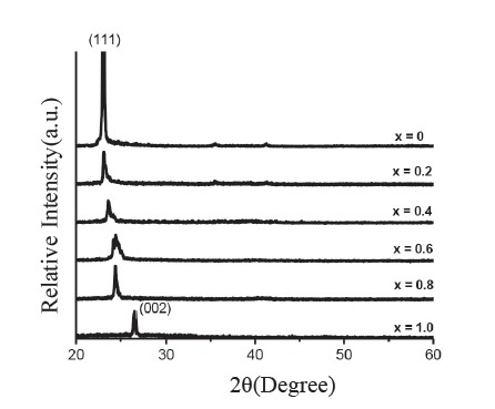
Figure 1. XRD patterns of CdSxTe1-x thin films.
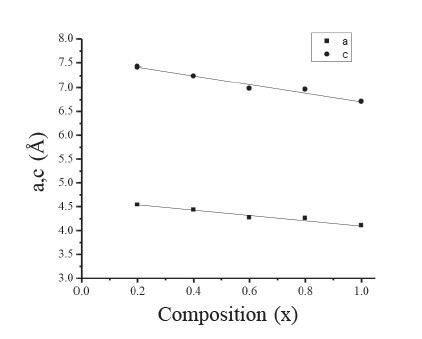
Figure 2. Variation of lattice constants a and c of CdSxTe1-x (0.2 ≤ x ≤ 1) thin films.
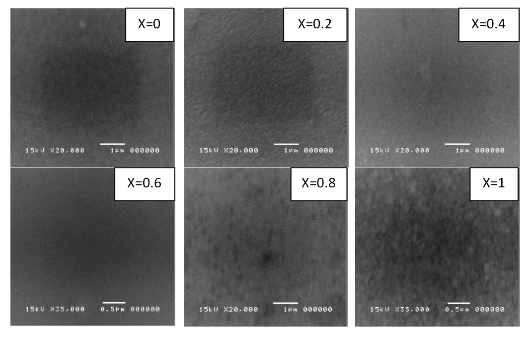
Figure 3. SEM images of CdSxTe1-x thin films.
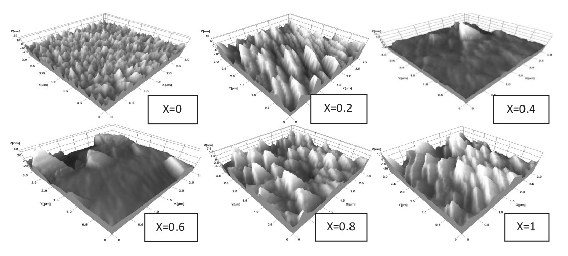
Figure 4. AFM images of CdSxTe1-x thin films.
The plot of percentage of transmittance as a function of the wavelength for the CdSxTe1-x thin films at various compositions (0 ≤ x ≤ 1) is shown in Figure 5. The spectra showed good transparency and interference patterns. The absorption edge gradually shifted to a shorter wavelength when composition (x) increased. The plots of (αhν)2 = A(hν - Eg) of the films with different compositions approximated a straight line, indicating that the optical transition in the films corresponded to the model for direct allowed transition. The value of the band gap is given by the intercept of the straight line with the energy axis. The band gap value decreased from 1.50 eV (corresponding to the Eg value of a CdTe single crystal) with increasing sulfur concentration, passing through a minimum value of 1.45 eV, and then increased to 2.40 eV (corresponding to the Eg value of a CdS single crystal). Figure 6 shows the composition dependence of the band gaps of the films.
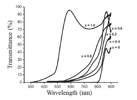
Figure 5. Transmittance of CdSxTe1-x thin films.
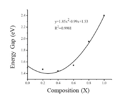
Figure 6. Variation of band gap of CdSxTe1-x thin films.
The photocurrent of the CdSxTe1-x thin films for x=0.8 is shown in Figure 7. The current immediately increased under illumination. When the illumination was switched off, the persistent photoconductivity (PPC) behavior of the films (for x=0.8) was observed. The decay of PPC seen in Figure 7 can be described by multiple exponential functions (Yadav et al., 2010; Jiang et al., 2011) as:

where Idark is the current measured in darkness, I0 is the PPC buildup level near the moment of light excitation being removed, and τ is the PPC decay time. The normalized decay current in darkness, as shown in Figure 8, which follows the illumination period, indicated the persistence of charge carrier traps in the films (Arslan et al., 2008). In Figure 8, the dashed line is the experimental data and the solid line is the least squares fit data from the multiple exponential functions described above. According to the function of fitting a curve in Figure 8, we calculated that the five τ values were 4.5, 24.6, 751.9, 1,879.3, and 5,963.0 s, respectively. The method for calculating the trap densities corresponding to the PPC decay constant has been reported in the literature (Studenikin et al., 1998; Gu et al., 2005; Huang and Lin, 2011). The corresponding trap densities were 7.68×10¹⁴, 2.47×10¹⁴, 1.68×10¹⁴, 1.47×10¹⁴ and 1.41×1014 cm-2, respectively.
Figure 9 shows the decay time of the CdSxTe1-x thin films for x = 0.8 performed at different temperatures. As Ip/(I0–Idark)=1/e, the corresponding t in equation (3) is equal to the time constant (τ). The τ is dependent on temperature. This behavior can be explained as the probability of the thermal activation of the localized carriers to overcome the potential barrier increases by way of increasing temperature. The potential barrier can be estimated from the temperature dependence of the time constant (Arslan et al., 2008) using the following equation:

where τ0 is the high temperature limit of the time constant and Ea is the activation energy for the thermal capture of an electron at its trap energy level. Figure 10 shows the plot of ln τ versus 1,000/T on the temperature dependence of PPC decay time. The linear fit in Figure 10 provides the activation energy of the electron trapping center of about 15 meV.
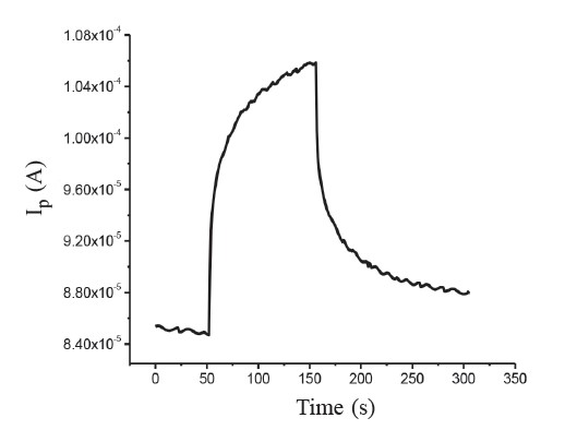
Figure 7. Photocurrent of CdSxTe1-x thin films for x=0.8.
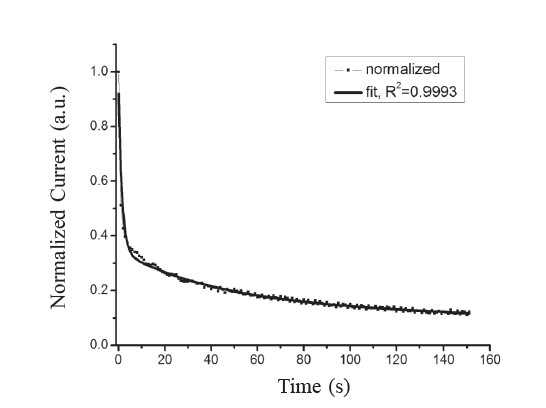
Figure 8. Normalized decay current of CdSxTe1-x thin films for x=0.8.
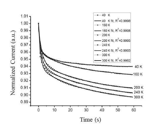
Figure 9. Temperature dependence decay time of CdSxTe1-x thin films for x=0.8.
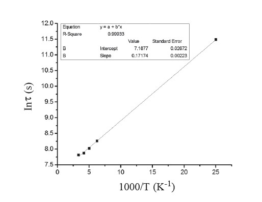
Figure 10. Arrhenius plot of decay time of CdSxTe1-x thin films for x=0.8.
DISCUSSION
For x˂0.2, XRD revealed that CdSxTe1-x thin films exhibited a cubic zincblende structure with the preferred orientation of (111) plane. However, for x ≥ 0.8, the films existed in the hexagonal wurtzite structure with the preferred orientation of (002) plane. For the composition 0.2 ≤ x ≤ 0.6, the cubic and the hexagonal phases coexisted in the system and the films became less preferentially oriented. The coexistence of the cubic and hexagonal phases often occurring in films with composition (x) in the range 0.2-0.8 has been previously reported (Wood et al., 1998; El-Nahaas et al., 2007; Al-Shakarchi, 2010). With increasing composition (x), the strongest peak intensity shifted to a higher 2θ value; this is due to the partial replacement of Te atoms by S atoms, indicating a reduction in the lattice constant. The lattice constants ‘a’ and ‘c’ varied linearly in accordance with Vegard’s law, corresponding to an earlier report (El-Nahaas et al., 2007).
From SEM micrographs, the average grain size of the CdSxTe1-x thin films increased by increasing the composition (x). AFM images of the films with composition x = 0 showed a polycrystalline character with pyramidal shaped crystallites, typical of cubic crystallites oriented in (111) plane. The grain size increased from 100 nm to 250 nm, as the value of x increased from 0 to 1. As composition (x) increased up to 0.4, the coexistence of flattening and pyramidal shaped crystallites was observed; this was consistent with the mixed phases seen in the XRD results. Then, a well-defined prism geometry was observed when x=1. The surface roughness decreased from 5.25 nm (for x = 0) to 3.24 nm (for x = 0.4), and then increased to 6.53 nm (for x=1). The variation of the direct band gap Eg (x) with composition (x) of the films is expressed conventionally in the quadratic form (Lane, 2006; Adachi, 2009; Hadrich et al., 2009):

where b is the direct band gap bowing parameter, Eg of CdS = 2.40 eV, and Eg of CdTe = 1.50 eV, corresponding to bulk semiconductors. The bowing parameter b=1.85 indicated an upward bowing of the band gap, which agreed well with the value reported elsewhere (Lane, 2006; Adachi, 2009).
The persistent photoconductivity effect has been observed in several materials including SnS (Jiang et al., 2011), Cu2ZnSnS4 (Jiang et al., 2012), AlGaN (Arslan et al., 2008), and ZnO (Yadev et al., 2010). PPC occurs because the photo-excited carriers are trapped and spatially separated by local potential barriers that inhibit the recombination of free carriers. The holes captured in the hole trap levels and the electrons captured in the electron trap levels cannot be released immediately. Thus, the excess electrons should stay in the conduction band and excess holes should stay in the valence band to maintain the electric charge neutrality. The recombination of excess carriers consists of two processes: recombination via electron and/or hole traps (assigned to process A) and direct recombination between the conduction and valence bands (assigned to process B). Since process B occurs quickly and process A takes longer, the direct recombination (process B) must take more time to preserve the electric charge neutrality. Thus, the excess carriers have a long lifetime, giving rise to a PPC effect.
The decay time of CdSxTe1-x thin films for x=0.8 performed at different temperatures leads to a time constant (τ) that is dependent on temperature. This behavior can be explained as the probability of the thermal activation of the localized carriers to overcome the potential barrier increases by way of increasing temperature.
In conclusion, CdSxTe1-x thin films were successfully prepared by a single-source thermal evaporation method using powder of pure CdS and CdTe compounds pressed in pellet form. Single phases with composition x<0.2 (CdTe-like) and x ≥ 0.8 (CdS-like) were obtained. However, for the composition 0.2 ≤ x ≤ 0.6, the cubic and hexagonal phases coexisted in the system and the films became less preferentially oriented. The optical transition in CdSxTe1-x thin films was of the direct allowed transition type. The variation of band gap (Eg) with composition (x) of the films is in good agreement with the quadratic form, giving a bowing parameter (b) = 1.85 eV. The decay current data were better fitted with multiple exponential functions. Five slow decay times and five trap densities values were obtained. The activation energy of the electron trapping center was about 15 meV.
In future research, we aim to clarify the behavior of the cubic and hexagonal coexistence phases in the CdSxTe1-x thin films by TEM.
ACKNOWLEDGMENTS
The authors would like to thank T. Wongcharoen and C. Poo-Rakkiat for valuable discussions. This study was supported by King Mongkut’s Institute of Technology Ladkrabang (Grant number A118-59-038).
REFERENCES
Adachi, S. 2009. Properties of semiconductor alloys group-IV, III-V and II-VI semiconductor (pp. 210-211). John Wiley & Sons, New York.
Al- Shakarchi, E.M. 2010. Phase transformation of a CdTe1-xSex thin films under an annealing process. Journal Korean Physics Society. 57: 1421-1425. https://doi.org/10.3938/ jkps.57.1421
Arslan, E., Butun, S., Lisesivdin, S.B., Kasap, M., Ozcelik, S., and Ozbay, E. 2008.The persistent photoconductivity effect in AlGaN/GaN heterostructures grown on sapphire and SiC substrate. Journal of Applied Physics. 103: 103701-7 - 103701-3. https://doi.org/10.1063/1.2921832
El- Nahass, M.M., Sallam, M.M., Afifi, M.A., and Zedan, I.T. 2007. Structural and optical properties of polycrystalline CdSxTe1-x (0 ≤ x ≤ 1). Material Research Bulletin. 42: 371-384. https://doi.org/10.1016/j.materresbull.2006.05.022
Gu, G., Kane, G., Doty, J.E, and Firester, A.H. 2005. Electron traps and hysteresis in pentacence-based organic thin film transistors. Applied Physics Letters. 87: 243512-1- 243512-3. https://doi.org/10.1063/1.2146059
Hadrich, M., Kraft, C., Metzer, H., Reislohner, U., Loffler, C., and Witthuhn, W. 2009. Formation of CdSxTe1-x at the p-n junction of CdS-CdTe solar cells. Physica Status Solidi. 6(5): 1257-1260. https://doi.org/10.1002/pssc.200881219
Huang, B.C., and Lin, Y.J. 2011. Effect of the induced electron traps by oxygen plasma treatment on transfer characteristics of organic thin film transistors. Applied Physics Letters. 99: 113301-1 - 113301-3. https://doi.org/10.1063/1.3636411
Ikhmayies, S.J. 2016. S-rich CdS1-yTey thin films produced by the spray pyrolysis technique. Energy. 9: 234-1-234-19. https://doi.org/10.3390/en9040234
Jiang, F., Shen, H., Gao, C., Liu, B., Lin, L., and Shen, Z. 2011. Preparation and properties of SnS films grown by two-stage process. Applied of Surface Sciences. 257: 4901-4905. https://doi.org/10.1016/j.apsusc.2010.12.143
Jiang, F., Shen, H., and Wang, W. 2012. Optical and electrical properties of Cu2ZnSnS4 films prepared by sulfurization method. Journal of Electronic Materials. 41: 2204-2209. https://doi.org/10.1007/s11664-012-2112-8
Lane, D.W. 2006. A review of the optical band gap of thin films CdSxTe1-x. Solar Energy Materials and Solar Cells. 90: 1169-1175. https://doi.org/10.1016/j.solmat.2005.07.003
Lane, D.W., Roger, K.D., Painter, S.D., Wood, D.A., and Ozsan, M.G. 2000. Structural dynamics in CdS-CdTe thin films. Thin Solid Films. 361-362: 1-8. https://doi.org/10.1016/S0040-6090(99)00827-5
Morales-Acevedo, A. 2006. Can we improve the record efficiency of CdS/CdTe solar cells? Solar Energy Materials and Solar Cells. 90(15): 2213-2220. https://doi.org/10.1016/ j.solmat.2006.02.019
Santana-Aranda, M.A., and Melendez-Lira, M. 2000. Structural and optical characterization of screen-printed CdSxTe1-x films. Superficies y Vacio. 10:36-39.
Studenikin, S.A., Geleco, N., and Cocivera, M. 1998. Optical and electrical properties of undoped ZnO films grown by spray pyrolysis of zinc nitrate solution. Journal of Applied Physics. 83(4): 2104-2111. http://dx.doi.org/10.1063/1.366944
Wood, D.A., Roger, K.D., Lane, D.W., Conibeer, G.J., and Parton, D. 1998. A study of the CdS-CdTe pseudobinary system. Journal of Material Science Letters. 17: 1511-1514.
Yadav, H.K., Sreenivas, K., and Gupta, V. 2010. Persistent photoconductivity due to trapping of induced charge in Sn/ZnO thin films based UV photodetector. Applied Physics Letters. 96: 223507-1- 223507-3. http://dx.doi.org/10.1063/1.3427417
Thitinai Gaewdang* and Ngamnit Wongcharoen
Department of Physics, Faculty of Science, King Mongkut’s Institute of Technology Ladkrabang, Bangkok 10520, Thailand
*Corresponding author. E-mail: thitinai.ga@kmitl.ac.th
Total Article Views

