 ISSN: 2822-0838 Online

Preparation of CuO Thin Films by Thermally Oxidized Metallic Cu Films for CdS/CuO Heterojunction Diode
Ngamnit Wongcharoen* and Thitinai GaewdangPublished Date : 2017-01-01
DOI : 10.12982/cmujns.2017.0006
Journal Issues : Number 1 ,January - March 2017
ABSTRACT
Copper thin films were deposited on glass substrates using thermal evaporation in vacuum and then thermally oxidized in air at temperatures of 100-500°C. XRD patterns showed the formation of a fine grain Cu2O phase at 300°C and a CuO phase at 400°C, respectively. Crystallinity and grain size improved with increasing oxidation temperature. The energy gap of the samples evaluated from absorption measurements was 2.10-2.23 eV. Important electrical parameters of the CuO thin films obtained from oxidizing at 500°C were resistivity of 8.53x10³ Ω•cm, carrier concentration of 7.60x1013 cm-3, and mobility of 6.22 cm2/V•s. A prototype of a CdS/CuO thin-film heterojunction diode was successfully prepared by thermal evaporation of CdS thin films on CuO thin-film substrate in a vacuum. The obtained device exhibited a good rectifying behavior from I-V characteristics. Junction parameters calculated using I-V data were barrier height of 5.190 eV, ideality factor of 0.520, and series resistance of 3.87 Ω. Impedance spectroscopy of the device was investigated at temperatures of 25-60°C. The real and imaginary parts of the complex impedance changed with the temperature and frequency. The experimental results suggested that the device was a good candidate for photovoltaic devices with low thermal budget and low product cost.
Keywords: CuO thin films, Thermal oxidation, CdS/CuO heterojunction, Impedance spectroscopy
INTRODUCTION
Copper oxides are semiconducting materials that have a natural abundance of starting material Cu. They have been extensively studied because of their potential applications in solar cells, gas sensors, electrochemical sensors, and batteries (Valladares, 2012; Ooi et al., 2013). Copper oxides are composed of two oxide phases, namely, cupric oxide (CuO) and cuprous oxide (Cu2O) with p-type conductivity; the former has a narrow band gap of 1.21-1.51 eV absorbing throughout the visible spectrum with a monoclinic structure, while the latter has a direct optical band gap of 2.10-2.60 eV with a cubic structure (Cho et al., 2013). A meta-stable copper oxide, Cu4O3, which is an intermediate compound between the previous two, has also been reported (Ooi et al., 2013). Numerous methods such as reactive sputtering, chemical vapor deposition, sol-gel, electro-deposition, and thermal oxidation have been used to grow copper oxide thin films. In this work, we investigated the effect of temperature of oxidation on the properties of copper oxide thin films prepared by oxidation of thermal vacuum evaporated Cu thin films. We studied the structural, optical, and electrical properties of the films to assess their potential use in p-n junctions. The formation of CdS/CuO heterojunction was elaborated by thermal evaporation of CdS thin films on CuO thin films coated on an ITO glass substrate. We investigated I-V and C-V characteristics of the CdS/CuO heterojunction to evaluate some important parameters, including junction barrier height, ideality factor, and series resistance values, by using thermionic emission theory and Cheung’s method. Moreover, impedance spectroscopy of the device was investigated at a temperature range of 25-60°C.
MATERIALS AND METHODS
Preparation and characterization of thin films for CdS/CuO diode
Copper thin films were grown on glass substrates by thermal evaporation in a vacuum better than 5x10⁻⁵ mbar. Before deposition, the glass substrates were cleaned in acetone, ethanol, and de-ionized water, in succession. The starting material was metallic Cu pellets (99.99% purity). The film thickness of about 200 nm was monitored by a quartz crystal thickness monitor (Edward type FTM 6). The thermal oxidation of Cu films was carried out in a muffle furnace at different temperatures, ranging from 100-500°C, for 60 min. The heating rate was maintained at 100°C/h. After soaking at the desired temperature for 60 min, the furnace was turned off, allowing the samples to cool to room temperature naturally. The crystal structure of these films was checked by X-ray diffraction technique with a Brucker D 8 diffractometer using CuKa radiation. Surface morphology was examined by a scanning electron microscope (JEOL model JSM-6400). A UV-VIS double beam spectrophotometer measured optical absorption in the wavelength range of 220-800 nm. The band gap (Eg) of the transparent films was determined by the equation (αhν)2 = Aʹ(hν-Eg), where α is the absorption coefficient, Aʹ is a constant, and hν is the photon energy. The absorption coefficient (α) was calculated
by using the relation α = 2.303A/d, where A is the absorbance and d is the thickness of the sample. The (αhν)2 data were obtained from optical absorbance measurements and, following the method reported by Tauc, were plotted as a function of photon energy (hν) to estimate the energy gap (Eg).
Electrical properties of the films were evaluated by Hall effect and resistivity measurements in the van der Pauw configuration at room temperature. To fabricate the CdS/CuO thin film heterojunction, Cu thin films were deposited on ITO-coated glass substrate and oxidized at 500°C for 60 min. CdS thin films were subsequently evaporated onto CuO films. Finally, an ohmic contact was made with silver paste on the surface of CdS and on the surface of ITO.
Electrical transport model
Based on the thermionic emission (TE) mechanism, current flows in a semiconductor diode is given by the relations (Rhoderick and William, 1988):
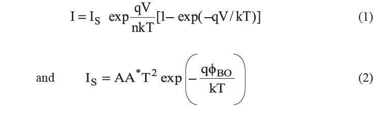
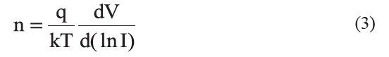
where IS is the saturation current derived from the straight line intercept of the semi-logarithmic I-V plot at V=0; V is forward bias voltage; T is the absolute temperature; q is the electronic charge; k is the Boltzmann constant; A is the effective area; A* = 4πqme/h3 is the effective Richardson constant of 20 A•cm-2• K-2 for n-CdS, where m*=0.165m0 is the effective mass of the electrons; ϕB0 is the apparent barrier height at zero bias voltage; and n is the ideality factor. Once IS is known from a least square fit of equation (1) to the linear part of the measured semi-logarithmic I-V plot, the zero bias barrier height (ϕB0) can also be computed with the help of equation (2). From equation (1), the ideality factor n is given by:
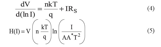
Cheung proposed an efficient technique to determine RS, n, and ϕB0 (Aksoy and Cagar, 2014). From equation (1), the following functions can be written as:
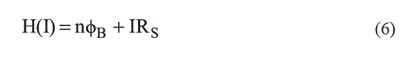
and H(I) is given as:
where ϕB0 is the barrier height obtained from data of downward curvature region in the forward bias I-V characteristics.
Electrical characterization of diode
The I-V characteristic curves were measured by a computer-interfaced Keithley 236 current/voltage source at room temperature. The bias voltage used was from -0.5 to 1.0 V. Impedance spectroscopy was carried out by Agilent E4980A Precision LCR Meter with frequency range of 10 kHz - 2 MHz and temperature range of 25-60°C.
RESULTS
Cu-O films characteristics
The XRD patterns of the as-grown and thermally oxidized Cu films at different temperatures ranging from 100-500°C are shown in Figure 1. The as-grown Cu sample revealed a diffraction peak at 2θ equal to 43.50° that corresponded to the (111) diffraction plane of metallic Cu. Oxidation of Cu thin films at 100 and 200°C still showed the purely (111) diffraction plane of metallic Cu phase, with reduction in peak intensity. For the sample Cu films oxidized at 300°C, a weak diffraction peak at 36.46° corresponding to the (111) plane of Cu2O was observed. However, at an oxidation temperature of 400°C, the (-111) diffraction plane of monoclinic CuO phase occurred. For the films oxidized at 500°C, two well-resolved diffraction peaks at 2θ of 35.40° and 38.35° were observed. These peaks correspond to diffraction of the (-111) and (111) planes of standard JCPDS data of CuO (JCPDS No. 80-1268). Figure 2 shows the SEM micrograph of Cu films oxidized at 100, 300, and 500°C. The surface of the as-deposited Cu films was mostly smooth and uniform, while the surface particle size and surface roughness
increased with increasing thermal oxidation temperature.
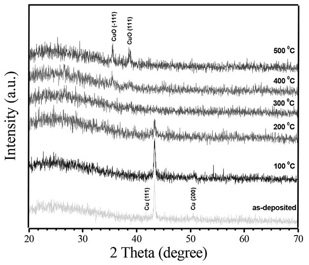
Figure 1. XRD patterns of CuO films.
Electrical properties of the films were evaluated by Hall effect and resistivity measurements in the van der Pauw configuration. Cu films oxidized at 100-500°C exhibited p-type conductivity. Variations of the resistivity (ρ), carrier concentration (p), and mobility (μ) against oxidation temperature are shown in Figure 3. The as-deposited and the Cu films oxidized at 100°C showed very low resistivity (~10-4 Ω•cm). In contrast, the films oxidized at temperatures beyond 200°C showed high resistivity, on the order of 103 Ω•cm. The carrier concentration initially decreased as the oxidation temperature increased up to 300°C, and then increased at higher oxidation temperatures. The mobility gradually decreased from 31.28 to 6.22 cm2/V•s as the oxidation temperature increased from 100 to 500°C.
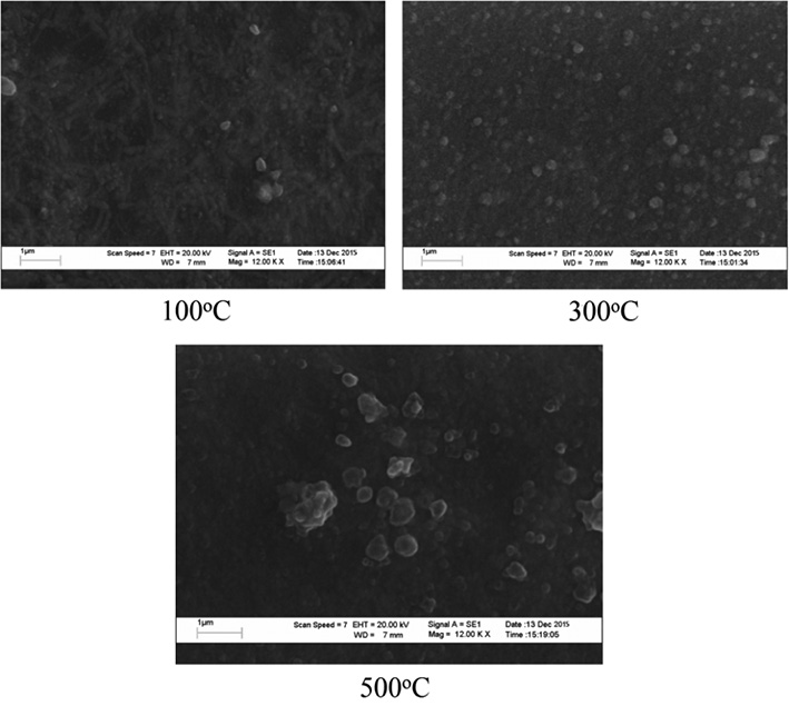
Figure 2. SEM micrographs of CuO films oxidized at 100, 300, and 500°C.
Figure 4 shows the absorbance (A) as a function of wavelength for the films oxidized at different temperatures. The absorbance value decreased as the wavelength increased. Figure 5 displays the plot of the energy gap of the films oxidized at 300°C calculated using Tauc’s method. Variation of energy gap as a function of oxidation temperature is shown in Figure 6. The Eg value initially increased up to the maximun value 2.23 eV at an oxidation temperature of 300°C, and then decreased to the minimum value 2.10 eV at 500°C.
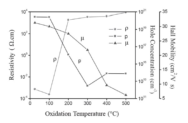
Figure 3. Variation of ρ, p, and μ of CuO films.
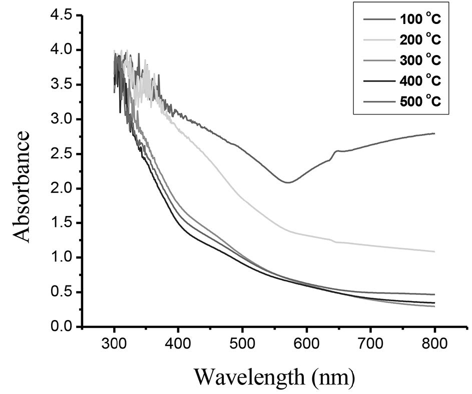
Figure 4. Absorption spectra of CuO films.
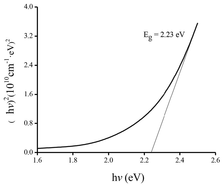
Figure 5. Plot of (αhν)2 vs. hν of CuO films oxidized at 300°C.
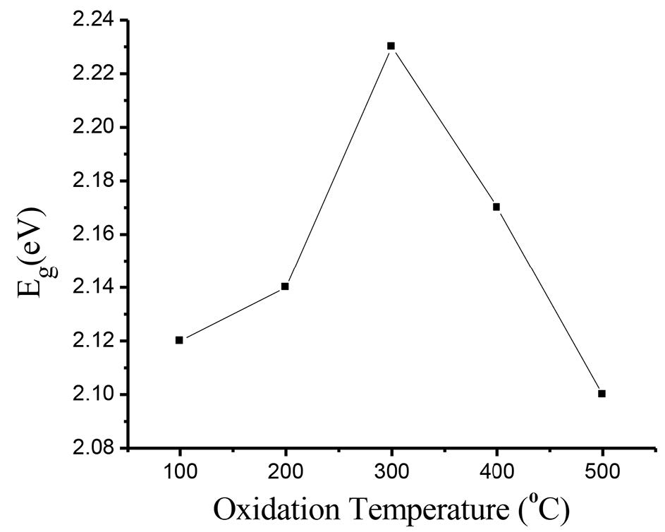
Figure 6. Variation of Eg with oxidation temperature.
Device characteristics
The measured I-V plot of CdS/CuO diode at room temperature is shown in Figure 7. Figure 8 shows the semi-logarithmic I-V plot within bias voltage of about 0.1-0.4 V. From Equations (2) and (3), the experimental value of the ideality factor and barrier height were 5.190 and 0.520 eV, respectively. The lnI-lnV plot is presented in Figure 9. According to Cheung’s model, the plots of dV/d(lnI) vs. I and H(I) vs. I are shown in Figures 10 and 11, respectively.
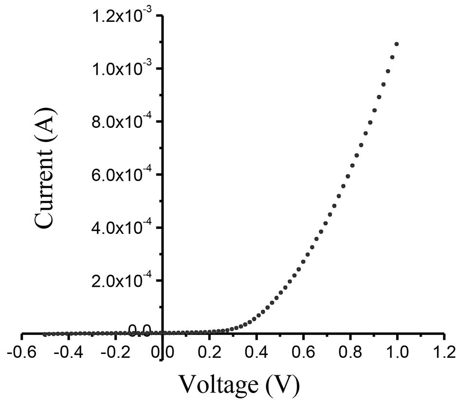
Figure 7. I-V plot of CdS/CuO diode.
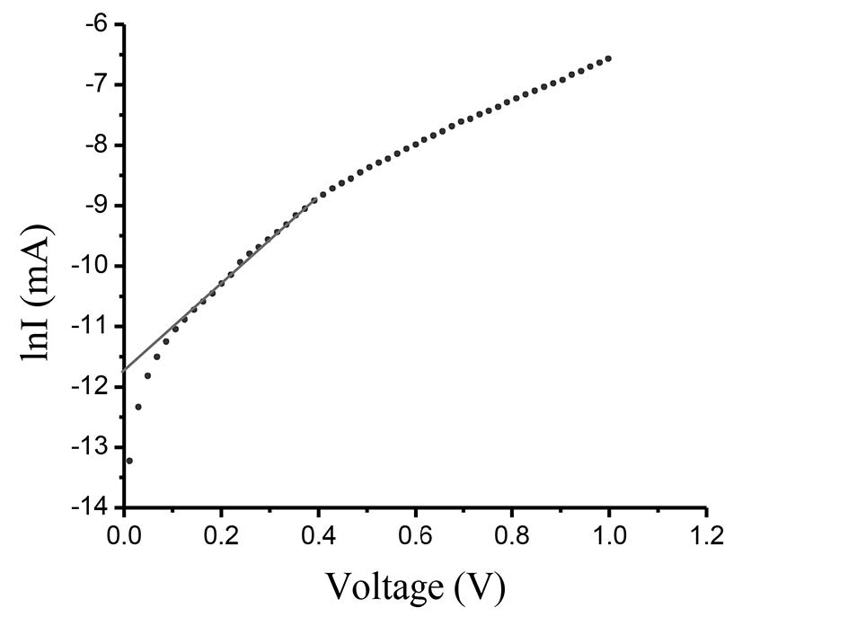
Figure 8. lnI-V plot of CdS/CuO diode.
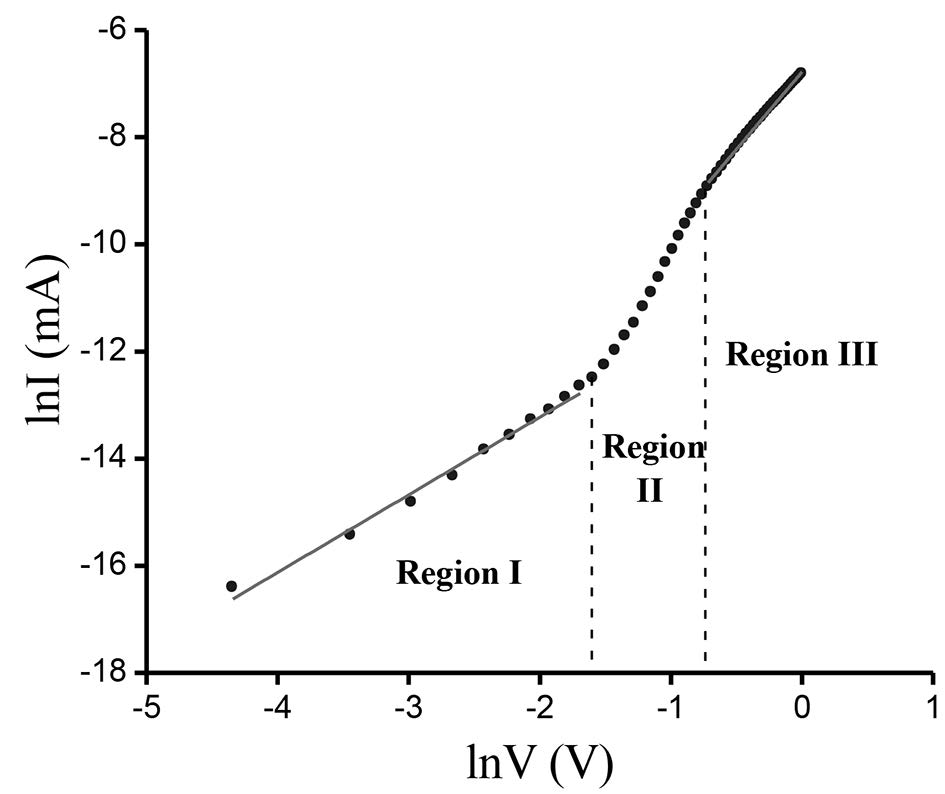
Figure 9. lnI-lnV plot of CdS/CuO diode.
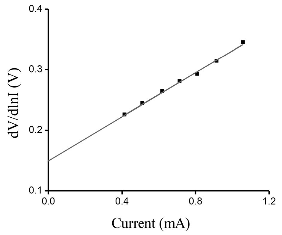
Figure 10. dV/d(lnI)-I plot of CdS/CuO diode.
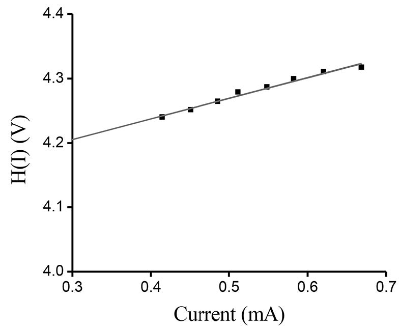
Figure 11. H(I)-I plot of CdS/CuO diode.
The variations in the real (Zʹ) and imaginary (Zʺ) parts of complex impedance with frequency at different temperatures are shown in Figures 12 and 13, respectively. The relaxation frequency (ω0) was obtained from the peak frequency of Zʺ-f plot. The Arrhenius plot of ln(ω0/T2) is shown in Figure 14.
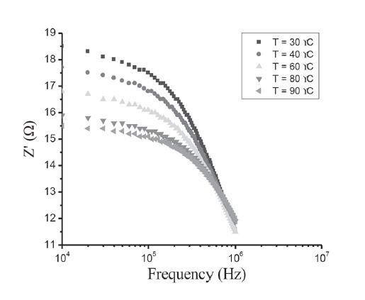
Figure 12. Zʹ-f plot of CdS/CuO diode.
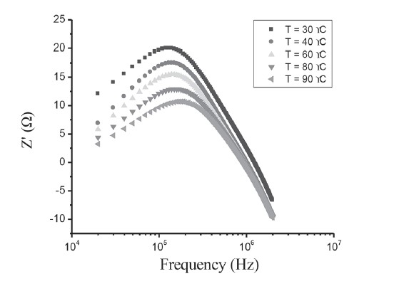
Figure 13. Z'-f plot of CdS/CuO diode.
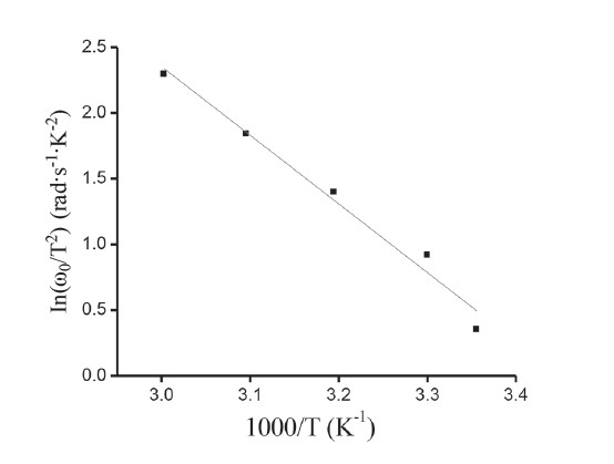
Figure 14. Arrhenius plot of ln(ω0/T2).
DISCUSSION
The as-grown CdS/CuO heterojunction showed a good rectifying behavior. The observed high ideality factor (>1) of the diode suggested that the thermionic emission model did not define well the device’s transport properties. To better understand the mechanism that controls the transport properties of this heterojunction, a lnI-lnV plot was presented. It is evident from the lnI-lnV plot that forward bias characteristics showed three regions. The I-V characteristics of region I (V<0.1V) complied with linear ohmic behavior (I~V), which is mainly caused by thermally generated charge carriers (Tyaki et al., 2015). In region II (0.1≤V≤0.4V), the current increased exponentially with bias voltage (I ~expαV). This is mainly due to the recombination-tunneling mechanism (Aksoy and Cagar, 2012). At higher bias voltage (region III, V>0.4V), the I-V characteristics followed a power law relation (I~V2). The current flow through the junction is due to space-charge limited current (SCLC) conduction, dominated by a single energy trap level (Zeyada et al., 2015). This SCLC mechanism is a normal phenomenon in a wide band gap semiconductor (Tyaki, 2015).
The series resistance (RS) is an important parameter in the electrical characteristics of a diode. This parameter is significant in the downward curvature (non-linear region) of the forward bias I-V characteristics; but the other two parameters (n and ϕB0) are significant in both the linear and non-linear regions of the I-V characteristics. Equation (4) should give a straight line for the data of the downward curvature region in the forward bias I-V characteristics. Thus, a plot of dV/d(lnI)-I will give RS as the slope and nkT/q as the y-axis intercept. The values of n and Rs were calculated as 5.322 and 3.48 Ω, respectively. This n value is slightly different from that obtained from the forward bias lnI-V plot. This difference may be caused by the presence of series resistance and interface states (Aksoy and Cagar, 2012). Using the n value determined from equation (4) and the data of the downward curvature region in the forward bias I-V characteristics in equation (5), a plot of H(I)-I should generate a straight line with the y-axis intercept equal to nϕB0. The slope of this plot also determines RS, which can be used to check the consistency of this approach. From Figure 11, the barrier height and series resistance of the device were calculated as 0.542 and 3.87 Ω, respectively. Furthermore, the values of RS obtained from the dV/d(lnI)-I and H(I)-I plots were in good agreement with each other, indicating the consistency of Cheung’s approach.
Figure 12 represents the variation of the real part (Zʹ) of complex impedance as a function of frequency at different temperatures. The variation shows two different frequency regions in which changes are visible with the change in temperature. For the low frequency range, there was a monotonous decrease in the value of Zʹ with an increase in temperature. This behavior changed drastically in the high frequency region, which showed a complete merger of the Zʹ plot above a certain frequency (~600 kHz). At a particular frequency, the magnitude of Zʹ decreased with increasing temperature. This is a typical behavior of semiconductor materials. The plot of Zʺ with frequency at various temperatures, as shown in Figure 13, revealed that Zʺ values reached a maximum before decreasing with further increases of the applied frequency, indicating a single relaxation process in the studied device. The relaxation frequency (ω0) corresponding to the Zʺmax shifted to higher frequency with increasing temperature. From the Arrhenius plot of ln(ω0/T2), activation energy of the deep traps occurring at the CdS/CuO junction was subsequently calculated as 0.466 eV. The appearance of a discrete trapping level was consistent with the results observed in dc transport studies corresponding to SCLC conduction controlled by a single energy trap level.
In conclusion, copper oxide thin films were obtained by thermal oxidation of Cu thin films prepared by thermal evaporation in a vacuum at temperatures beyond 200°C. From the XRD patterns, the films oxidized at 500°C showed a pure CuO phase. The surface particle size and surface roughness increased with increasing thermal oxidation temperatures. A CdS/CuO heterojunction was successfully fabricated by thermal evaporation of CdS thin films on CuO thin films obtained by oxidation at 500°C for 60 min. Three types of transport mechanisms controlled fabricated by thermal evaporation of CdS thin films on CuO thin films obtained by oxidation at 500°C for 60 min. Three types of transport mechanisms controlled the forward current transport, namely: Ohmic conduction, recombination-tunneling, and space-charge limited current mechanisms, depending on the applied forward bias voltage. The real and imaginary parts of the complex impedance changed with the temperature and frequency. The experimental results suggested that the photovoltaic properties of the heterojunction diode should be studied further, as well as their potential use in photovoltaic devices with low thermal budget and low product cost. the forward current transport, namely: Ohmic conduction, recombination-tunneling, and space-charge limited current mechanisms, depending on the applied forward bias voltage. The real and imaginary parts of the complex impedance changed with the temperature and frequency. The experimental results suggested that the photovoltaic properties of the heterojunction diode should be studied further, as well as their potential use in photovoltaic devices with low thermal budget and low product cost.
ACKNOWLEDGMENTS
The authors would like to thank Assoc. Prof. Dr. T. Wongcharoen and Asst. Prof. Dr. C. Poo-Rakkiat for their valuable input. This work was supported by King Mongkut’s Institute of Technology Ladkrabang (grant number 2558A11802069/164817).
REFERENCES
Aksoy S., and Y. Cagar. 2012. Effect of ambient temperature on electrical properties of nanostructure n-ZnO/p-Si heterojunction diode. Superlattices and Microstructures. 51: 613-625. doi: 10.1016/j.spmi/.2012.02.018.
Aksoy, S., and Y. Cagar. 2014. Structural transformation of TiO2 films with deposition temperature and electrical properties of nanostructure n-TiO2/p-Si heterojunction diode. Journal of Alloys and Compounds. 613: 330-337. Doi: 10.1016/j.jallcom.2014.05.192.
Barsoukov E., and J.R. Macdonald. 2005. Impedance Spectroscopy: Theory, Experiment and Application. 2nd Ed., John Wiley & Sons, New York.
Cho, S. 2013. Optical and electrical properties of CuO thin films deposited at several growth temperatures by reactive rf magnetron sputtering. Metals and Materials International. 19: 1327-1331. doi: 10.1007/s12540-013-6030-y.
Ooi, P.K., S.S. Ng, M.J. Abdullah, H. Abu Hassan, and Z. Hassan. 2013. Effect of oxygen percentage on the growth of copper oxide thin films by reactive radio frequency sputtering. Materials Chemistry and Physics. 140: 243-248. doi:10.1016/j.matchemphys.2013.03.028.
Rhoderick, E.H., and R.H. William. 1988. Metal-Semiconductor Contacts. 2nd Ed., Oxford University Press.
Tyagi M., H. Toman, and V. Gupta. 2015. Trap assisted space charge conduction in p-NiO/n-ZnO heterojunction diode. Material Research Bulletin. 66:123-131. doi: 10.1016/j.materresbull. 2015.02.015.
Valladares L.L.S., D.H. Salinas, D.A. Najarro, S.I. Khondake, T. Mitrelias, C.H.W. Barnes, J.A. Aguiar, and Y. Majima. 2012. Crystallization and electrical resistivity of Cu2O and CuO obtained by thermal oxidation of Cu thin films on SiO2/Si substrates. Thin Solid Films. 520: 6368-6371. doi: 10.1016/j.tsf.2012.06.043.
Zeyada H.M., M.M. El-Nahass, E.M. El-Menyawy, and A.S. El-Sawah. 2015. Electrical and photovoltaic characteristics of indium phthaloyanine chloride/p-Si solar cell. Synthetic Metals. 207: 46-53. doi: 10.1016 /j.synthmet.2015.06.008.
Ngamnit Wongcharoen* and Thitinai Gaewdang
Department of Physics, Faculty of Science, King Mongkut’s Institute of Technology
Ladkrabang, Bangkok 10520, Thailand
*Corresponding author. E-mail: ngamnit.wo@kmitl.ac.th
Total Article Views